NPTH
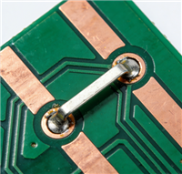
Non plated though-hole.
Non-wetting
A condition whereby a surface has contacted molten solder, but has had none of the solder adhere to it.
Non-polar Compound
Material having electrical charges distributed over the surface of the molecule, thereby showing an electrical effect in solution.
Non-functional Land
A land on internal or external layers, not connected to the conductive pattern on its layer.
Non-conductive Pattern
A configuration formed by functional non-conductive material of a printed circuit.
Non-conductive Epoxy
An epoxy resin with or without a filler, which may be added to improve thermal conductivity.
Non-clean solder
A process using specially formulated low-solid solder pastes whose residues require no cleaning.
Node
A pin, lead or even junction which will have at least one wire connected to it.
NFP
Non-functional pad.
Neutralizer
An alkaline chemical added to water to improve its ability to dissolve flux residues.
Netlist
A net is a junction of component nodes. A netlist is a collection of nets that define all the connections in a circuit. It is obtained automatically from a schematic capture program.
Negative–acting Resist
A resist which is polymerized (hardened) by light and which, after exposure and development remains on the surface of a laminate in those areas which were under the transparent parts of a production ,master.
Negative (Noun)
An artwork, artwork master, or production master in which the intended conductive pattern is transparent to light, and the areas to be free from conductive material are opaque.
Nail Heading
The flared condition of copper on the inner conductor layers of a multi-layer board usually caused by hole drilling.


