Prototipos de PCB de forma sencilla

Servicio completo para prototipos de PCB personalizados.

Centro de Ayuda
Enviando un mensaje
9:00 - 23:00, Mon.- Sun. (GMT+8)
Líneas directas de servicio
+86 571 8531 7532

9:00 - 18:00, Mon.- Fri. (GMT+8)

9:00 - 12:00, Sat. (GMT+8)

(Excepto los días festivos chinos públicos)

Archivos necesarios para PCBA

Listado de materiales (BOM) en formato CSV o Excel
Gerbers en formato RS274X para las capas de cobre, serigrafía y pasta de soldadura
Archivo “Pick and place” o XYRS (Pick-n-place, localización de componentes, o X, Y, rotación, datos de lado – Centroide de los componentes)

Archivos necesarios para PCBA

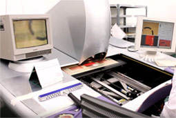
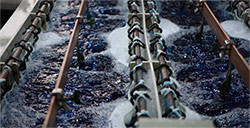
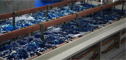
El montaje de PCBs necesita de algunos archivos para que podamos comenzar el trabajo de PCBA. Por favor, envíenos los siguientes archivos en el formato adecuado. Tendrá dos opciones para enviarnos esos archivos, el primero es a través de nuestra página en línea, el Segundo es enviarlo mediante correo electrónico a es-service@pcbway.com poniendo como referencia su número de pedido en el tema del mensaje como “Archivos para el pedido número 123456”

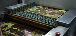
BOM (Listado de materiales)

BOM es la lista de componentes utilizados en la fabricación de los productos finales. Muestra qué components son necesarios para montar las placas, y dónde deben colocarse y montado. Aceptamos archivos BOM en los formatos .xls, xlsx o .csv. El BOM para pedidos completes y parciales quizá necesite aportar más información que el BOM para pedidos consignados o en kit.Aquí están los detalles.

BOM para pedidos consignados/en kit puede incluir la siguiente información::
  • Línea#
  • Cantidad por referencia de componente
  • Referencia
  • Número de componente
  • Descripción del componente
  • Empaquetado
  • Tipo (montaje superficial, pasante o híbrido)
BOM para pedidos completos o parciales puedeincluir la siguiente información:
  • Línea#
  • Cantidad por componente
  • Referencia
  • Número de componente
  • Descripción del componente
  • Empaquetado
  • Tipo (montaje superficial, pasante o híbrido)
  • Nombre del fabricante
  • Número de componente del fabricante
  • Número de componente del distribuidor
Pulse para descargar un ejemplo de BOM
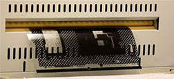
Archivos Gerber

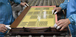
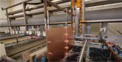
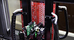
Parta montar sus placas se necesitarán los mismos archivos Gerber en formato RS-274X que nos envió para la fabricación de sus PCBs. Como mínimo, el montador de PCB necesitará archivos de tres capas: serigrafía, cobre (pistas) y máscara de soldadura. Asegúrese de que todos esos archivos han sido revisados e incluidos por su parte. Por supuesto que nosotros también revisaremos esos archivos antes del montaje para asegurarnos de que toda la información está completay es precisa.

Archivo centroides

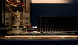
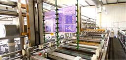
El archivo de centroides es un archivo especial para el montaje, utilizado para programar rápidamente las máquinas de montaje. Esto también se conoce como inserción, “Pick-N-Place”, o datos XY. Algunas de las herramientas de CAD generan automáticamente este archivo y otras no, pero quizá necesite modificar el archive y generar después el archive de centroides. El archive de centroides describe la posición y orientación de todos los componentes de montaje superficial, lo que incluye la referencia, posiciónX e Y, rotacióny lado de la placa (superior o inferior). Solo se listan componentes de montaje superficial en el archive de centroides.

Pulse para descargar un archivo de centroides de ejemplo

Otros

Para que podamos montarcorrectamente sus placas de circuito impreso, le recomendamos encarecidamente que nos envíe todos los demás documentos e información relativa a las placas, lo que puede incluir los dibujos de montaje, instrucciones de montaje especiales, e incluso imágenes o fotos de su trabajo. Esta información nos ayuda a entender mejor sus necesidades de montaje, corrigiendo algunos posicionamientos ambiguos o incluso erróneos, y finalice con un trabajo excelente. Envíelos, aunque no sean necesarios generalmente por los Montadores.

Contáctenos!

Nuestro servicio de atención al
cliente preparado para su PCB

+86-571-85317532

quotesI am impressed with the quality of the boards, the delivery time and responce to all my questions. Best price excellent service and speedy delivery. When I need another board I will certainly use this supplier. "

-Bill Robinson Company

quotesспасибо за платы! платы очень хорошего качества. надежный продавец. оперативно отвечал на вопросы. заказ выполнили и отправили очень быстро.Заказываю платы не в первый раз - как всегда только лучшие впечатления. 5+++. 4 числа отправил файлы 26-го забрал на почте в Москве."

-FVL. SKU Company
Front-end data preparation

01.PPE - Pre Production Engineering

Customer supplied data (gerber) is used to produce the manufacturing data for the specific PCB (artworks for imaging processes and drill data for drilling programs). Engineers compare demands/specifications against capabilities to ensure compliance and also determine the process steps and associated checks. No changes are allowed without PCBWay Group permission.

Preparing

02.Preparing the phototools

Artwork Master is PCB production in the key steps, which directly affect the quality of the final product quality,An accurately scaled configuration of electronic data used to produce the artwork master or production master. Artwork Master – The photographic image of the PCB pattern on film used to produce the circuit board, usually on a 1:1 scale.In general, there are three types of Artwork Master:(1) Conductive Pattern  (2) solder mask (3) Silkscreen

print icon

03.Print inner layers

Stage 1 is to transfer the image using an artwork film to the board surface, using photosensitive dry-film and UV light, which will polymerise the dry film exposed by the artwork.
This step of the process is performed in a clean room.
Imaging – The process of transferring electronic data to the photo-plotter, which in turn uses light to transfer a negative image circuitry pattern onto the panel or film.

etch icon

04.Etch inner layers

Stage 2 is to remove the unwanted copper from the panel using etching. Once this copper has been removed, the remaining dry film is then removed leaving behind the copper circuitry that matches the design.
Etching – The chemical, or chemical and electrolytic, removal of unwanted portions of conductive or resistive material.

aoi icon

05.Inner layer Automatic Optical Inspection(AOI)

Inspection of the circuitry against digital “images” to verify that the circuitry matches the design and that it is free from defects. Achieved through scanning of the board and then trained inspectors will verify any anomalies that the scanning process has highlighted. PCBWay Group allows no repair of open circuits.

Lamination icon

06.Lay-up and bond (Lamination)

The inner layers have an oxide layer applied and then “stacked” together with pre-preg providing insulation between layers and copper foil is added to the top and bottom of the stack. The lamination process consists of placing the internal layers under extreme temperature (375 degrees Fahrenheit) and pressure (275 to 400 psi) while laminating with a photosensitive dry resist. The PCB is allowed to cure at a high temperature, the pressure is slowly released and then the material is slowly cooled.

drilling icon

07.Drilling the PCB

We now have to drill the holes that will subsequently create electrical connections within the multilayer PCB. This is a mechanical drilling process that must be optimised so that we can achieve registration to all of the the inner layer connections. The panels can be stacked at this process. The drilling can also be done by a laser drill

copper icon

08.Electroless copper deposition

The first step in the plating process is the chemical deposition of a very thin layer of copper on the hole walls.
PTH provides a very thin deposit of copper that covers the hole wall and the complete panel. A complex chemical process that must be strictly controlled to allow a reliable deposit of copper to be plated even onto the non-metallic hole wall. Whilst not a sufficient amount of copper on its own, we now have electrical continuity between layers and through the holes.Panel plating follows on from PTH to provide a thicker deposit of copper on top of the PTH deposit – typically 5 to 8 um. The combination is used to optimise the amount of copper that is to be plated and etched in order to achieve the track and gap demands.

image icon

09.Image the outer layers

Similar to the inner layer process (image transfer using photosensitive dry film, exposure to UV light and etching), but with one main difference – we will remove the dry film where we want to keep the copper/define circuitry – so we can plate additional copper later in the process.
This step of the process is performed in a clean room.

Plating icon

10.Plating

Second electrolytic plating stage, where the additional plating is deposited in areas without dry film (circuitry). Once the copper has been plated, tin is applied to protect the plated copper.

etch icon

11.Etch outer layer

This is normally a three step process. The first step is to remove the blue dry film. The second step is to etch away the exposed/unwanted copper whilst the tin deposit acts an etch resist protecting the copper we need. The third and final step is to chemically remove the tin deposit leaving the circuitry.

AOI

12.Outer layer AOI

Just like with inner layer AOI the imaged and etched panel is scanned to make sure that the circuitry meets design and that it is free from defects. Again no repair of open circuits are allowed under PCBWay demands.

Soldermask

13.Soldermask

Soldermask ink is applied over the whole PCB surface. Using artworks and UV light we expose certain areas to the UV and those areas not exposed are removed during the chemical development process – typically the areas which are to be used as solderable surfaces. The remaining soldermask is then fully cured making it a resilient finish.
This step of the process is performed in a clean room.

Surface finish

14.Surface finish

Various finishes are then applied to the exposed copper areas. This is to enable protection of the surface and good solderability. The various finishes can include Electroless Nickel Immersion Gold, HASL, Immersion Silver etc. Thicknesses and solderability tests are always carried out.

Profile

15.Profile

This is the process of cutting the manufac-turing panels into specific sizes and shapes based upon the customer design as defined within the gerber data. There are 3 main options available when providing the array or selling panel – scoring, routing or punching. All dimensions are measured against the customer supplied drawing to ensure the panel is dimensionally correct.

Electrical test

16.Electrical test

Used for checking the integrity of the tracks and the through hole interconnections – checking to ensure there are no open circuits or no short circuits on the finished board. There are two test methods, flying probe for smaller volumes and fixture based for volumes.We electrically test every multilayer PCB against the original board data. Using a flying probe tester we check each net to ensure that it is complete (no open circuits) and does not short to any other net.

inspection

17.Final inspection

In the last step of the process a team of sharp-eyed inspectors give each PCB a final careful check-over.Visual checking the PCB against acceptance criteria and using PCBWay “approved” inspectors. Using manual visual inspection and AVI – compares PCB to gerber and has a faster checking speed that human eyes, but still requires human verification. All orders are also subjected to a full inspection including dimensional, solderability, etc.

Packaging

18.Packaging

Boards are wrapped using materials that comply with the PCBWay Packaging demands (ESD etcetera) and then boxed prior to be being shipped using the requested mode of transport.