During the design and manufacturing process of PCB, there may be some factors such as material properties, manufacturing processes, environmental factors, etc., which may cause changes in the electrical characteristic parameters of the PCB, and finally affect its performance. Therefore, corresponding compensation measures need to be taken to ensure the stability and reliability of PCB.
Below are some common production compensation used by PCBWay in PCB production.
Trace Compensation
The Reason for Trace Width Compensation
After electroplating, the trace is etched using a trace etching machine. Due to the thickness of the trace, vertical etching (commonly called side etching) will also occur during horizontal etching. Therefore, in order to compensate for side etching, the trace needs to be compensated. The side etching is shown in the following figure:

The Industry Standard of Trace Width Compensation
The compensation for 1oz copper thickness:

Compensation can cause some issues. For example, if the spacing between the original line and the copper foil is 4 mil, the trace needs to be compensated on one side by 0.3 mil, and the left side copper foil also needs to be compensated by 0.3 mil. Then the actual spacing after compensation would be 4mil-0.3mil-0.3mil=3.4mil. However, 3.4mil is smaller than the production process capability, which for regular boards at PCBWay is 6mil.

At this point, the engineer will remove the left side copper foil because they believe that reducing the left side copper foil slightly will not significantly affect the trace, and it is more important to ensure the integrity of the independent trace on the right side. As a result, the file provided by the customer has been modified.
Drill Compensation
The Reason for Drill Compensation
The hole size specified in the Gerber files provided by the customer typically refers to the finished hole size. However, during PCB production, copper plating (or surface treatment such as immersion gold, OSP, or immersion tin) is applied inside the hole, resulting in a reduction of the hole size. In order to ensure that the finished hole size meets the requirements, drill compensation will be performed to correct the hole size.
For example, if the customer requires a final finished hole size (defined in the PCB design software as the drilled hole size) of 1.00mm, with immersion gold (nickel thickness: 2.54um, gold thickness: 0.0254um), IPC standard Class II (average hole copper: 20um), and a 0.15mm compensation for the hole size, the engineering department will select a 1.15mm drill bit to drill the holes.

2.The Industry Standard for Drill Compensation

The compensation value depends on the compensation value rules established based on the factory's production capacity test results. The drilling compensation values in the entire industry are generally similar.
Pad Compensation
When designing pads on a PCB surface, taking into account the errors in the manufacturing process, the size and shape should be adjusted to match the components, and finally achieve reliable connections and excellent electrical performance.
Pad compensation is an important step in PCB manufacturing, aiming to improve the quality and reliability of soldering. Due to factors such as temperature, pressure, and material during PCB production, the actual size and shape of the pads may differ from the design. If compensation is not performed, it may result in loose connections, poor soldering quality, or even soldering failure.
Generally, there are several methods for pad compensation:
a. Diameter compensation: Adjusting the diameter of the solder pad to match the component, typically increasing or decreasing the diameter by no more than 10% based on the actual situation.
b. Shape compensation: Adjusting the shape of the solder pad, such as changing from a circular pad to a square or elliptical pad, or adding protrusions or indentations to the pad's edge to change its shape.
c. Spacing compensation: Adjusting the distance between adjacent pads, typically not less than 1.2 times the width of the component's pins.
During pad compensation, it is important to consider soldering processes, component pin spacing, and PCB design to ensure reliable connections and high-quality soldering.
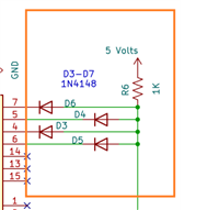
Pad compensation may cause a series of issues, as shown in the following figure:

According to PCBWay's manufacturing capabilities, it is recommended that the spacing between pads for BGA and IC should not be less than 0.15mm. If the spacing is less than 0.15mm, solder pad compensation will be performed to try to avoid short circuits and meet production requirements.

The effect after cutting is shown below:

Material Compensation
Material compensation in the production process of PCBs is a crucial step, aimed at compensating for material expansion, contraction, and other issues that may arise during PCB manufacturing. This is done to ensure that the dimensions and shape of the PCB remain stable throughout the manufacturing process.
Generally speaking, material compensation needs to consider the following aspects:
a. Thermal expansion coefficient of materials: Different types of PCB materials have different thermal expansion coefficients, which will affect the size and shape of the PCB. Therefore, in the production process of PCBs, it is necessary to compensate for the size of the PCB based on the thermal expansion coefficient of the selected material, to ensure that the size and shape of the PCB can remain stable during production.
b. The selection of size and material of the printed circuit diagram: The size and material of the printed circuit diagram also affect the size and shape of the PCB. Therefore, in the production process of the PCB, it is necessary to consider the size and material of the printed circuit diagram and make appropriate compensation according to the actual situation.
c. Control of manufacturing process parameters: In the production process of PCBs, it is necessary to control manufacturing process parameters such as temperature, humidity, heating time, etc., to ensure that the size and shape of the PCB remain stable during the manufacturing process. At the same time, it is also necessary to adjust different manufacturing process parameters to meet the manufacturing requirements of different types of PCBs.
In summary, material compensation is an important step that requires a comprehensive consideration of factors such as substrate material, printed circuit diagram dimensions and material selection, and manufacturing process parameters to ensure the stability of PCB dimensions and shape during the production process.
Electrical Characteristic Compensation
The electrical characteristics of the PCB, such as impedance and capacitance, may be affected by factors such as the routing of the trace, the board material, and the vias. Therefore, appropriate compensation measures need to be taken to ensure the performance of the PCB.
Electrical characteristic Compensation mainly includes the following aspects:
a. Resistance compensation: Resistance is one of the most basic electrical characteristic parameters in PCB circuits. In the design and manufacturing process of PCBs, the resistance value may be affected by various factors, such as substrate materials, trace width, trace spacing, wiring method, etc. To ensure the performance of the circuit, appropriate compensation measures need to be taken for the resistance.
b. Capacitance compensation: Capacitance is another important electrical characteristic parameter in PCB circuits. In the design and manufacturing process of PCBs, the capacitance value may be affected by various factors, such as substrate materials, trace width, trace spacing, trace length, wiring method, etc. To ensure the performance of the circuit, appropriate compensation measures need to be taken for the capacitance.
c. Signal delay compensation: Signal delay refers to the time required for a signal to be transmitted in a PCB circuit. In the design and manufacturing process of PCBs, the signal delay value may be affected by various factors, such as substrate materials, trace width, trace spacing, trace length, wiring method, etc. To ensure the timing performance of the signal, appropriate compensation measures need to be taken for the signal delay.
d. Impedance matching compensation: Impedance matching refers to matching the output impedance of the signal source with the input impedance of the load to achieve the best signal transmission effect. In the design and manufacturing process of PCBs, the impedance matching value may be affected by various factors, such as trace width, trace spacing, wiring method, etc. To ensure the impedance-matching performance of the signal, appropriate compensation measures need to be taken for the impedance.
In summary, compensating for PCB electrical characteristics is one of the important measures to ensure stable and reliable PCB circuit performance. In the design and manufacturing process of PCBs, it is necessary to comprehensively consider the electrical characteristic parameters and make appropriate compensations based on actual situations to ensure stable and reliable circuit performance.
It should be noted that different compensation measures may affect each other during PCB production. Therefore, it is necessary to consider comprehensively and make reasonable design and adjustment based on practical application scenarios and manufacturing costs.