Summary: Utilising the experience and services of PCBWay to define the critical characteristics and manufacture a flexible circuit design, here is a method for creating large Flexible PCB designs using two free tools Design Spark PCB and Gerbv.
Flexible circuits can offer a number of advantages over rigid PCBs being not only very thin but can include connection systems and cables as one single assembly. They can also be formed into the housing or simply used to provide a very thin substrate. They generally consist of layers below, built up and bonded with epoxy:
Overview of Flexible PCB technology is shown on the PCBWay blog. Pricing of Flexible circuit manufacture has reached a level that means it is more accessible to smaller businesses and adventurous hobbyists.
They are more difficult to design, features have to be large in size to ensure robustness and traces need to be curved to prevent stress fractures. They are not straightforward to develop using free tools, as free tools lack certain features to manage the complexities; Coverlays, copper features used to ensure a rugged design and conductive patterns for items such as switches.
A Worked Problem
This guide shows a worked design example, sponsored by PCBWay, of a very long and specialised flexible circuit used in a Music Synthesizer keyboard. In this design, it has 2 copper layers with vias, soldered surface mount components, double switch contacts and nearly 1 meter long. The contact arrangement is designed to be used with a rubber membrane switch contact array with carbon pips. There are two sets of contacts per key in order for the processor to measure velocity. In the original part it has carbon coatings instead of gold plating to keep costs low, however, they can oxidise over time and stop working properly. The picture below shows a section of the original failed green flexible circuit from an instrument.

The switch contacts and FPC connector make the design immediately problematic for a low feature count CAD tool; the solder resist output can’t be used to generate the Coverlay because it has to be excluded from the switch contact area.
Concept Design
An overview of the general characteristics and a concept design is first created. It is important to decide on a large and robust feature size for tracks, vias and component pads.


The properties of the design require research, there are many sites out there that explain the design rules for flexible circuits. However to speed up the process and validate the planned design, a good place to start is from an online quotation tool, where critical parameters may be manipulated and important choices made that infer the design characteristics.
Starting Point
First assessment involves the choice of connector, in this design a high quality and rugged 1mm pitch Molex 522072460 24Way top contact gold plated connector is chosen. It is essential to choose a high quality established part otherwise there will be problems, gold plating is essential and zero insertion force type prevents damage to the Flexi on insertion.
The construction and stack up of the layers is critical for the connector, as it has a very tight tolerance. The rest of the design will follow the stack up around the connector as it has a wide tolerance and keeping consistent stack up across the design ensures a cost effective design and manufacturing process.

Define Layer Stack Up
At this point a stack up was defined using Excel that is able to conveniently add up the various layer thicknesses and produce a total. Once complete, the main characteristics of the Flexi are completely defined. Note that an unconnected bottom layer copper section is defined for the FPC connector, this acts as a filler to meet the thickness requirements (300um +/-5). In this case, 2 um of ENIG plating is defined to ensure robustness and a few mating cycles. For many mating cycles “hard gold” is best utilised. The musical keyboard “push” switch contacts should be considered too, ENIG is softer but more resistant to corrosion, sometimes fluid can splash in between the keys so a thick layer of plating is useful for the switch contacts to be able to tolerate some level of cleaning if serviced.

Design Tool Issues & Workarounds
The free version of DesignSpark PCB is an excellent tool for designing PCBs, it has a number of limitations however when working with Flexible PCBs but they can be overcome with careful workaround and use of a Gerber file editor such as “Gerbv” available on the Linux platform:
Workarounds for these properties are managed carefully:
Creating Components
It is vital that your own library of components is created. If using component library databases such as SamacSys copy the component parts you need and make your own with the necessary modifications.
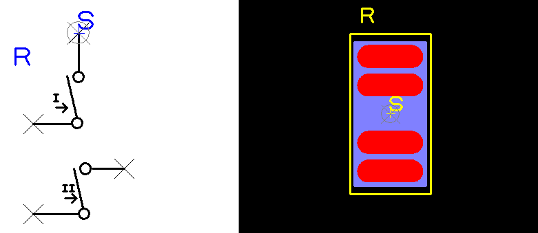
The switch contact has pads and a documentation layer to define where the Coverlay aperture lies. In this example it is important that the switch membrane pads do not catch the edge of the Coverlay when operated as they may result in a bad connection.
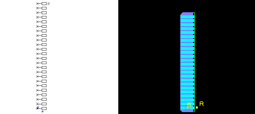
The FPC connector is created with the documentation layer showing the exclusion of Coverlay film plus a copy of the top copper layers if required to meet a defined stack up.
Create fixings and other components used in the design as you would in a normal PCB. For stack ups that have a deep Coverlay, it may be necessary to define an exclusion area in each part using the documentation layer (for example the switch components in this example) so that the body of the component can sit flush to the film and not lift the legs off the pads. Many small power diode packages have this property and can cause re-flow soldering issues.


Coverlay Design
In above examples, it is important to remember that the Coverlay is not just to resist solder but to provide mechanical strength to prevent tracks and pads from peeling off when flexed. The components above are defined for a flexible circuit in a “static” application, ie. flexed only during final assembly.
For applications that have regular flexing then other measures are necessary. One such feature is a “spur”. This can be done by adding tracks manually to the design across each pad, however they fail design rule checks or even the tool prevents placement. This example does not contain this feature, as it is a “Static Application”, ie. once assembled in product it does not flex. Some attempt was made to try and add these features to components themselves, but the tool seemed limited to one pad per connection with no overlaps and no extra copper allowed.
Design The Layout
The design is now undertaken after entering the schematic. Making connectivity mistakes with Flexible Circuits has a very high cost associated as they are extremely difficult to rework or modify. Even for simple circuits, it is therefore strongly recommended to not move directly to a layout but create a linked schematic too, so that all the circuit nodes and design rules can be verified.
In an excerpt for the design below, curved traces, large clearances and features are used to ensure robustness during handling. Copper traces did not sit directly above each other either, thus ensuring minimal strain when flexed. Tracks were 0.8mm and Vias with 1.2mm pads / 0.5mm holes.
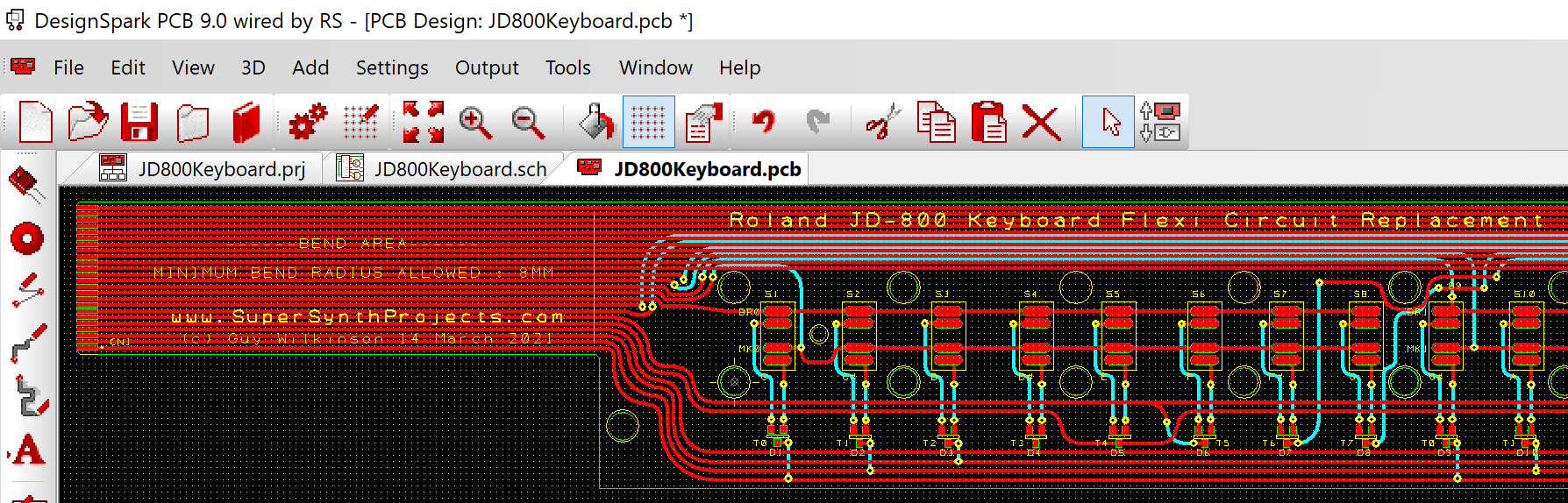
In this particular design, placement of components and fixing was notably painful, requiring tolerance of +/-0.1mm across the 1 meter length. The underlying metalwork, fixings and placement of switches is critical to ensure that the mechanical sub-assemblies fit correctly and do not affect the playing experience or missing notes! This design will need a lot of testing, study and design adjustments to ensure success.
Stiffener Design & Coverlay Data
It is essential to create a copy of the PCB that has two board outline regions defined for the Stiffener regions and a Soldermask with the vias removed. This was done by using “Save As”, once system and relative origins were set to a known fixing point on the PCB. In this case the bottom left fixing point on S1 was chosen and marked accordingly.
As the Coverlay data is generated from the Soldermask output (with documentation layer merged) and the via holes are generated at same time. It is necessary to remove the vias and their pads somehow. The process of removing the unwanted vias on the derived design is then performed manually as shown below.

Once completed the “child” design is minus any via holes and the two stiffener regions can be seen as separate board outlines.

Manufacturing Information
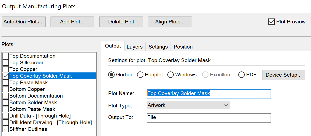
The next step is to create manufacturing information for the Top Coverlay and Stiffner outlines.
The Top Documentation layer containing additional Coverlay aperture information is turned on for the Top Solder Mask. The Top Solder Mask is also renamed to “Top Coverlay Solder Mask” to avoid confusion and a new plot “Stiffener Outlines” is created that is simply the board outlines.

It can be seen from the preview that the Coverlay is now generated correctly.

In the original board layout, generate the remaining manufacturing Gerber files using the normal methods in accordance with your designed stack up and fine naming convention.
Note that it is also important to provide a drawing to explain these characteristics and ensure that they are not overlooked by the manufacturer.
Gerber File View & Edit
It is now time to edit the Solder Paste file and check the generated files in a Gerber file viewer. First load the files into Gerbv and check alignment of the layers and that they do what you need represented.
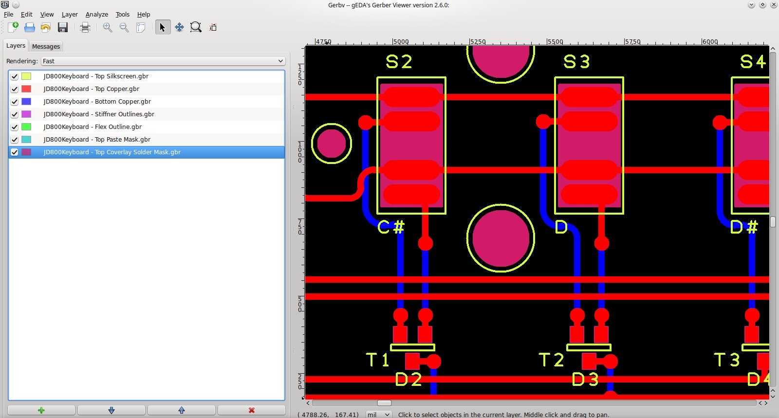
The hole placements can be checked too, simply load them into the viewer. Also a good idea to confirm that the via features are missing from the top and bottom Coverlays.
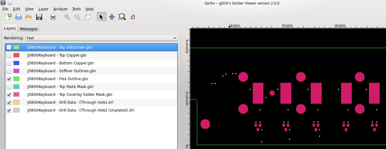
Select the Solder Paste Mask and delete the FPC and switch contact elements from the design.

It is done!
Gerbv now represents the manufacturing CAD data as you want it. All that is required now are the drawings that describe the characteristics, stack up and dimensional properties. It is vital to represent a picture of what you require so that the essential properties may be checked at the factory by QA personnel.
Original content Copyright © 2021 Super Synth Projects, Guy Wilkinson.


