Single-layer PCBs and double-layer PCBs are two basic types of boards that have only one or two layers of conductive materials over the substrate. When more routing space or signal integrity is required, multi-layer PCBs are suited to meet these demands. Unlike single-layer and double-layer PCBs, multilayer PCBs stack multiple layers of conductive and insulating materials to create a complex network of connections. The stack-up typically includes copper layers, cores, substrates, and prepreg. Prepreg and core are two types of insulating materials or dielectric materials in PCBs.
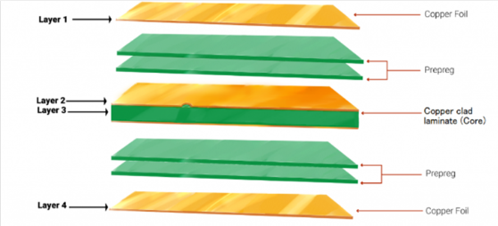
Figure1 : Multilayer PCB stack-up
What is prepreg?
Prepreg, short for pre-impregnated, is a layer of fiberglass cloth impregnated with uncured epoxy resin but without any attached copper foil. In a PCB stack-up, prepreg serves as both an insulating layer and an adhesive layer. When constructing a PCB stack-up, the prepreg is placed between adjacent copper layers or between a copper layer and a core material. During the manufacturing process, high temperature and pressure cause the epoxy resin in the prepreg to flow and bond the layers together, resulting in a solid, rigid board.
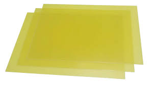
Figure2 : Prepreg
What is a core of a PCB?
The core of a PCB is the central layer of the board that provides mechanical support and rigidity. It typically consists of a laminate material made of thin layers of copper foil bonded to a rigid substrate material. The copper foil on the core can serve multiple purposes, such as providing a ground plane or a signal plane. In multilayer PCBs, there can be multiple core layers, with prepreg layers between each core layer and the outer copper layers.
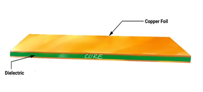
Figure3 : PCB core
HDI Stack-up
Compared to traditional PCB stack-ups that rely on through-hole vias to interconnect layers, HDI stack-ups utilize micro-vias, blind vias, and buried vias to achieve higher routing density and better electrical performance. The X-N-X structure is a common way to describe the HDI stack-up configuration. Here, X represents the number of HDI layers with micro-vias, while N represents the number of core layers sandwiched between these HDI layers. Some common stack-up configurations include 1-N-1, 2-N-2, and 3-N-3.
To further illustrate how the X-N-X structure is applied in practice, let's consider the example of a 1-4-1 stack-up configuration. In a 1-4-1 structure, there is one HDI layer with micro-vias at the top of the PCB, followed by four core layers with no micro-vias in between, and finally another HDI layer with micro-vias at the bottom of the PCB.
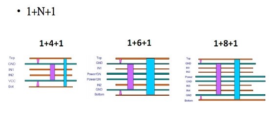
Figure4:HDI Stack-up example


