1. Blog>
  2. The PCB Assembly Process

The PCB Assembly Process

by: Sep 21,2018 11014 Views 4 Comments Posted in PCB Assembly

PCB Assembly SMT Assembly Adhesive Dispense Component Placement AOI Reflow Soldering

Introduction

With the rapid development of the modern information industry, electronic products are constantly improving and updating. Any electronic product cannot be separated from printed circuit board, which is the support body of electronic components and the provider of electrical connection of electronic components. High-density electronic product assembly on PCB is mainly dependent on SMT process. The rapid development and popularization of SMT---an important component of electronic advanced manufacturing technology has transformed the concept of traditional electronic circuit assembly and also created basic conditions for the miniaturization and lightweight of electronic products, becoming one of the indispensable technologies for manufacturing modern electronic products.

image.pngimage.png

About PCBWay: Just like PCB business, our PCBA services also specialize in prototyping and small-volume production, making PCBWay the one-stop destination of PCB fabrication and assembly. This arrangement makes your R&D work easy and time-saving. Our professional engineers and technicians will work closely with you through our customer service people to ensure the best quality and quickest possible lead time. Fulfilling thousands of orders daily from around the world, we have established us as the leading supplier of PCB and PCBA services for our consistent quality and excellent services.


PCBWay PCBA capabilities: SMT Assembly, BGA Assembly, Through-Hole Assembly, Mixed Assembly, Rigid Flex PCB Assembly Services. Compliant with a wide range of standards including IPC 610 Class 2 and Class 3.

image.png

RequiredElements

The following are the required elements for auto assembly:

·Gerbers in 274-X (embedded apertures) including fabrication drawing.

·Part centroid text file with Reference Designators, external placement layer, and X & Y location and rotation in ASCII format.

·Numerical control (NC) drill files

·Solder paste file (one of the Gerber files) for all sides mounted

·Glue dot file

·If possible, the design database, specifying the database format (program name)

·Parts list or BOM (bill of material)

·Parts or hardware required

Process of SMT (Video)

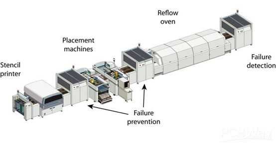
The simple process of SMT described below is for reference only:


Step 1. Printing:

Use solder paste printing press which is located at the end of the production line to print solder paste or patch adhesive onto PCB's solder pad to prepare components for welding.

image.png

Step 2. Adhesive Dispense:

This process is to use the glue dispenser which is mainly used for precise spot injection of glue paint and other liquids to the precise position of each product to drop the glue on the fixed position of PCB, and its main function is to fix the components to PCB when wave solder is used.

image.png


Step 3. Component Placement:

Once the printed PCB has been confirmed to have the correct amount of solder paste applied it moves into the next part of the manufacturing process which is component placement. Each component is picked from its packaging using either a vacuum or gripper nozzle, checked by the vision system and placed in the programed location at high speed. There is a large variety of machines available for this process and it depends greatly on the business to what type of machine is the assembly process, potentially reducing assembly costs.

image.png

Step 6. Post-Reflow Automated Optical Inspection (AOI):

The last part of the surface mount assembly process is to again check that no mistakes have been made by using an AOI machine to check solder joint quality. Sometimes, the movement during the reflow process will result in poor connection quality or a complete lack of a connection, in other words, shorts are also a common side effect of this movement, as misplaced components can sometimes connect portions of the circuit that should not connect. Thus, the inspection after reflow soldering is quite important and checking for these errors and misalignments can involve one of several different inspection methods. The most common of these inspection methods include the following:

Manual Checks

Automatic Optical Inspection(AOI)

Automated X-ray inspection(AXI)

image.png

Step 7. Conformal Coating:

Conformal coating material is a thin polymeric film which ‘conforms’ to the contours of a printed circuit board to protect the board's components. Typically applied at 25-250 μm(micrometers) thickness, it is applied to electronic circuitry to act as protection against moisture, dust, chemicals, and temperature extremes that, if uncoated (non-protected), could result in damage or failure of the electronics to function. When electronics must withstand harsh environments or impact, protection is provided with conformal coatings or potting compounds. Most circuit board assembly houses coat assemblies with a layer of transparent conformal coating, which is lighter and easier to inspect than potting.

image.png

Step 8. Final Inspection and Functional Test:

After the soldering and conformal coating step of the PCB assembly process is finished, a final inspection will test the PCB for its functionality by our Quality Assurance team. This inspection is known as a "functional test". The test software and tools are usually provided by the customer, PCBWay can also make fixtures according to customer requirements. The test puts the PCB through its paces, simulating the normal circumstances in which the PCB will operate. Power and simulated signals run through the PCB in this test while testers monitor the PCB's electrical characteristics.

image.png

Step 9. Washing & Drying:

Actually, there will be oil and dirt in the whole production process, so we need to clean and dry the PCB before it goes out. Fox example, soldering paste leaves behind some amount of flux, while human handling can transfer oils and dirt from fingers and clothing to the surface of the board.


Step 10. Packaging & Shipping:

All assembled boards are packaged (can request in anti-static packaging) and shipped DHL, FedEx, UPS, EMS, and so on. Any unused components are returned in accordance with customer instructions. Additionally, customers are notified via email when their packages ships.

image.png

Join us
Wanna be a dedicated PCBWay writer? We definately look forward to having you with us.
  • Comments(4)
You can only upload 1 files in total. Each file cannot exceed 2MB. Supports JPG, JPEG, GIF, PNG, BMP
0 / 10000
    Back to top