As the electronic products become thinner and smaller, the thickness and volume of PCB installed in these devices are smaller, which promotes the gradual maturity of HDI technology, resulting in ultra-thin and high-density HDI board. This kind of board has smaller volume, larger hole density and more dense lines, which is similar to the carrier board. As a high-difficult processing technology, the PCB board has the characteristics of ultra-thin, miniaturization, high density and high precision, which is also close to the limit of PCB design and production.
This ultra-thin and high-density HDI multi-layer plate is made by the laminated pressing of universal FR4 resin system plate, semi-curing plate and electrolytic copper foil. The control difficulties are the laminated pressing of ultra-thin core plate, mechanical drilling, laser drilling, and the expansion and contraction of ultra-process capacity core plate. A series of problems such as plate deformation, uncontroled thickness, and large interlayer deviation are easy to occur in the production and processing.
Product introduction:
Four-layer first-order HDI ( 1 + 2 + 1 ).
The thickness of the finished plate is 0.25mm + / -0.025mm.
Minimum mechanical pass 0.1 mm, 282038 holes.
Minimum laser hole 0.1 mm, hole 1345698 ( two sides ).
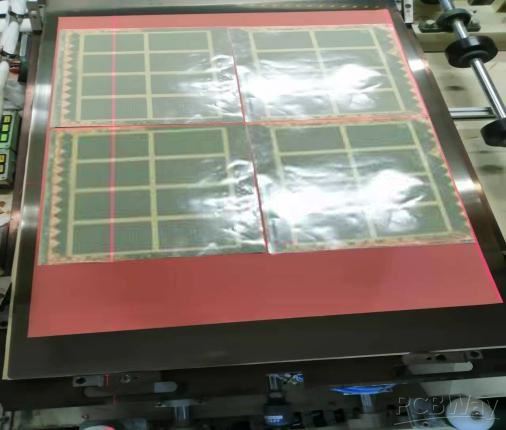
Single size 5 * 5mm, 546pcs per set ;
Internal drilling:
The number of holes is 282038, the thickness of the core plate is 0.065mm ( without copper ). After opening, the copper should be reduced to 7-9um. The minimum drilling tool in the inner layer is 0.1mm, and the customized drilling nozzle is used. The phenolic pad is used to avoid the lance and the plate deformation.
Laminate pressure:
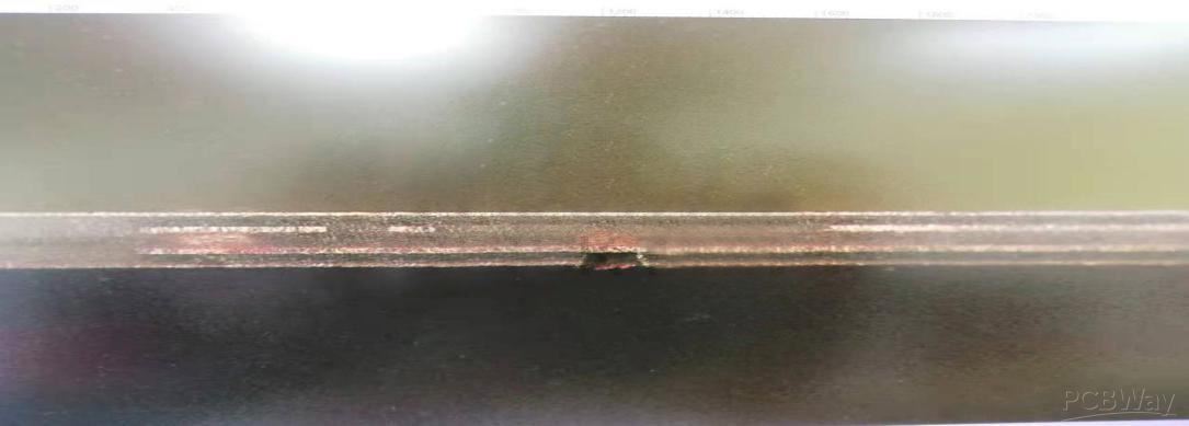
Pressing thickness 0.22 mm, single piece 106 P, layout 4pnl / layer, control the lack of glue and shrinkage. Laminate thickness and effect

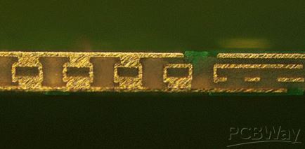
Laser drilling:
Laser hole density is very large, T surface 428241 holes, B surface 917457 holes, aperture 0.1 mm, outer single 106 PP inner core plate 0.065 mm copper thickness 18um, need to adjust the laser energy control laser breakdown and laser hole type, laser effect:
Electroplated plug holes and surface copper:
Because the thickness of the plate is 0.25mm and the thickness of the outer copper layer is not more than 18um, the laser hole needs to be filled with a baffle.
Soldermask:
Pad is small, sodermask needs to be made by LDI, and the surface treatment is made of nickel palladium gold process.
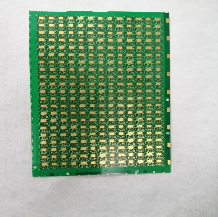
Product display:
The thickness of each layer of the product:
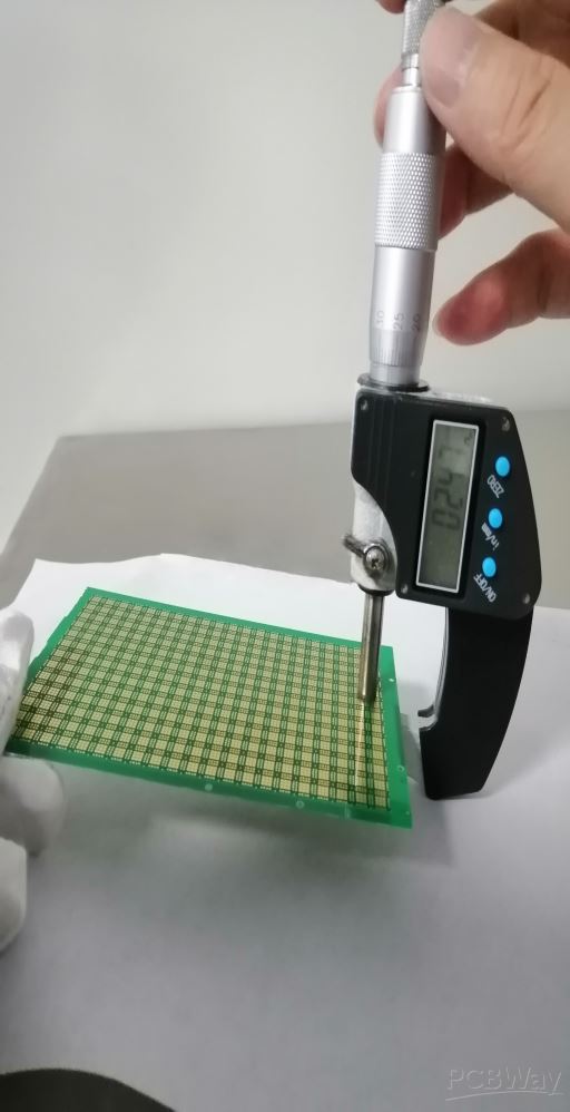
The thickness of the final finished plate is 0.247 mm:
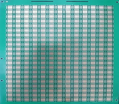
The appearance of the finished product: